![]()
![]()
Product Overview

I. Product Definition
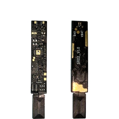
The Smart Ring Main Control PCB with NFC Antenna is the core component of a smart ring within wearable electronic devices. It is specifically designed to enable Near Field Communication (NFC), health monitoring, and smart interaction functionalities within the limited space of a wearable device. Its core architecture consists of an NFC antenna, a main control chip (MCU), sensor interfaces, and a power management module. It utilizes flexible multilayer PCB or rigid-flex PCB technology, with thickness controllable within 0.3-0.8mm, and diameter adaptable to the ring's inner diameter (typically less than 20mm).
The Smart Ring Main Control PCB with NFC Antenna is a miniaturized PCB assembly based on ultra-thin flexible copper-clad laminate (FCCL) combined with high-frequency substrate materials. It achieves high-density integration of the NFC antenna and main control chip through processes such as blind and buried vias and Laser Direct Imaging (LDI). Its core lies in employing a double-layer spiral coil antenna topology and a π-type impedance matching network to ensure communication stability in the 13.56MHz frequency band. Through a rigid-flex structure, it adapts to the curved form of the ring. It requires strict LCR parameter testing, resonant frequency calibration, and bend reliability validation to meet the comprehensive demands of wearable devices for extreme space constraints, low power consumption, and multi-scenario protocol compatibility (e.g., payment, access control).
II. Product Characteristics
The Smart Ring Main Control PCB utilizes an ultra-thin flexible substrate as its core carrier. Through composite design with high-frequency CCL and nanocrystalline absorbing materials, it achieves stable RF performance at the 13.56MHz band with a Q factor >30 and read/write distance ≥4cm. Using blind and buried vias (diameter ≤0.1mm) and LDI process, it accomplishes high-density integration of the double-layer NFC spiral antenna and the main control chip, achieving a trace density of up to 100 lines/mm². Simultaneously, it adapts to the ring's curved form via a rigid-flex structure (bend radius <0.3mm). It integrates dynamic impedance matching algorithms and a low-power power management module, resulting in standby current <10μA. Reliability is validated through 1000 bend cycle tests, meeting the comprehensive needs of wearable devices for miniaturization, anti-interference, and extended battery life.
III. Product Technical Support
The Smart Ring Main Control PCB requires efficient integration of RF communication, data processing, and power management within an extremely small space. Its technical support system centers on innovations in high-frequency RF materials, miniaturized circuit integration processes, and flexible structure design. Using a composite of ultra-thin flexible substrates and nanocrystalline absorbing materials enables low loss and anti-metal interference capability in the 13.56MHz band. Blind/buried vias and LDI processes achieve high-density interconnection (trace density ≥100 lines/mm²) between the NFC antenna and the main control chip. Combined with a Rigid-Flex structure (bend radius <0.3mm), it adapts to the curved form. Integrated dynamic impedance matching algorithms and low-power management modules ensure communication stability across the full temperature range (-40°C to 85°C). A reliability validation system based on 1000 bend cycles and salt spray tests enables a breakthrough in comprehensive performance encompassing miniaturization (diameter <20mm), ultra-long battery life, and multi-protocol compatibility (payment/access control).
Characteristic Material Technologies:
Stable relative dielectric constant (Dk);
Low coefficient of thermal expansion (CTE);
Characteristic Process Technologies:
Controllable trace width;
Controllable trace spacing (clearance);
Component/Assembly Technologies:
LCR Parameter and Impedance Matching Technology (Design & Manufacturing);
Coupling Enhancement and Shape Optimization Technology (Design & Manufacturing);
Antenna Size and Structural Design Technology (Design & Manufacturing);
IV. Product Manufacturing Process
Double-sided FCCL + Coverlay cutting, CNC drilling, Black Hole (or similar direct metallization process), plating, pattern transfer, exposure & development & etching, lamination, pressing, testing, etc.
V. Key QC Processes
Hole wall thickness/plating quality control;
Conductor (Trace) Defect Testing;
LC Circuit Performance Testing;
VI. Product Test Report
"Smart Ring Main Control PCB with NFC Antenna LCR Performance Test Report";
VII. Direct Product Assembly: Smart Ring Main Control Module

The Smart Ring Main Control Module is the core component within a smart ring. It employs advanced integration technology to highly integrate a low-energy Bluetooth (BLE) chip, NFC module, and health sensor interfaces. Paired with a flexible PCB design, it achieves an ultra-compact structure. It supports health functions such as heart rate, blood oxygen, and sleep monitoring, as well as smart operations like touch control, gesture recognition, and voice interaction. It is also compatible with wireless charging and medical-grade data accuracy, meeting the needs of all-day health management and convenient living within a lightweight wearing experience.
VIII. Final Product Assembly: Smart Ring
The following text and image provide a basic description of the smart ring.

A smart ring is a wearable device that integrates micro-sensors, wireless communication, and AI technology, focusing on health monitoring and convenient interaction. Its core functions include real-time heart rate, blood oxygen, and sleep quality tracking; some products support NFC payments, gesture control, and female physiological cycle management. Design emphasizes lightweight construction (e.g., 2-3 grams) and imperceptible wear, using skin-friendly materials like titanium alloy, with battery life reaching 7-15 days. Representative products include the Samsung Galaxy Ring (medical-grade data monitoring), RingConn (sleep apnea warning), and competing products under development by Apple. They are expanding health management scenarios through medical certification and AI integration.
Product Parameters
Product Stack-up Structure (Diagram):

Holes (PTH/NPTH): 0.15mm
Conductors/Traces: Line Width 0.09mm / Spacing (Clearance) 0.08mm
Solder Mask & Silkscreen (Legend): Solder Mask Opening (SMO): 2.710.71mm; Silkscreen Line Width: 0.13mm; Silkscreen Character Height: 0.83mm
Finished Product Dimensions: 39*6.5mm
Surface Finish: ENIG (Electroless Nickel Immersion Gold)
Defect Testing:
Trace Defects - AOI (Automated Optical Inspection) Testing
LCR Testing
Functional Testing:
Trace & Hole Open/Short Circuit Testing
Assembled/Component Testing (Functional Circuit Performance Testing):
《Smart Ring Main Control PCB with NFC Antenna LCR Performance Test Report》
Reliability Testing:
Thermal Shock Test
Product-Related Certification Pre-Testing:
Not Applicable (N/A) at this time
Product Unit Drawing:

 Download